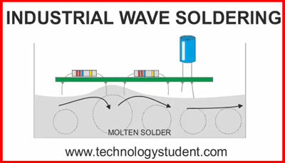
Wave soldering of circuits / PCBs (Printed Circuit Boards), is an industrial mass production process, capable of soldering high numbers of circuit boards in a short time. It also produces a high standard of solder joint, which results in a reliable, working circuit.
The process is relatively straightforward:
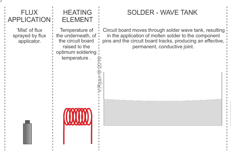
1. The clean circuit board with its components in position, is placed on a production line. The first stage is the application of flux. This is a substance that helps to keep the circuit board clean, by preventing oxidisation, during the heating process. The flux is sprayed in the form of a fine mist, onto the underneath of the board, covering the tracks and exposed ‘pins’ of the components.
2. The circuit board then moves to the next stage, where a heating element heats it to the optimum ‘soldering’ temperature, controlled precisely by sensors.
3. The circuit board then moves through the solder wave tank. The tank contains molten solder, which is formed into a ‘travelling’ wave. The wave makes contact with the underneath of the circuit board, joining the component pins to the tracks, producing an electrically efficient and permanent joint.
4. The circuit board is then allowed to cool, as it moves along the production line.
After manufacture, the circuit boards are checked for conductivity and that they are defect free and work properly.